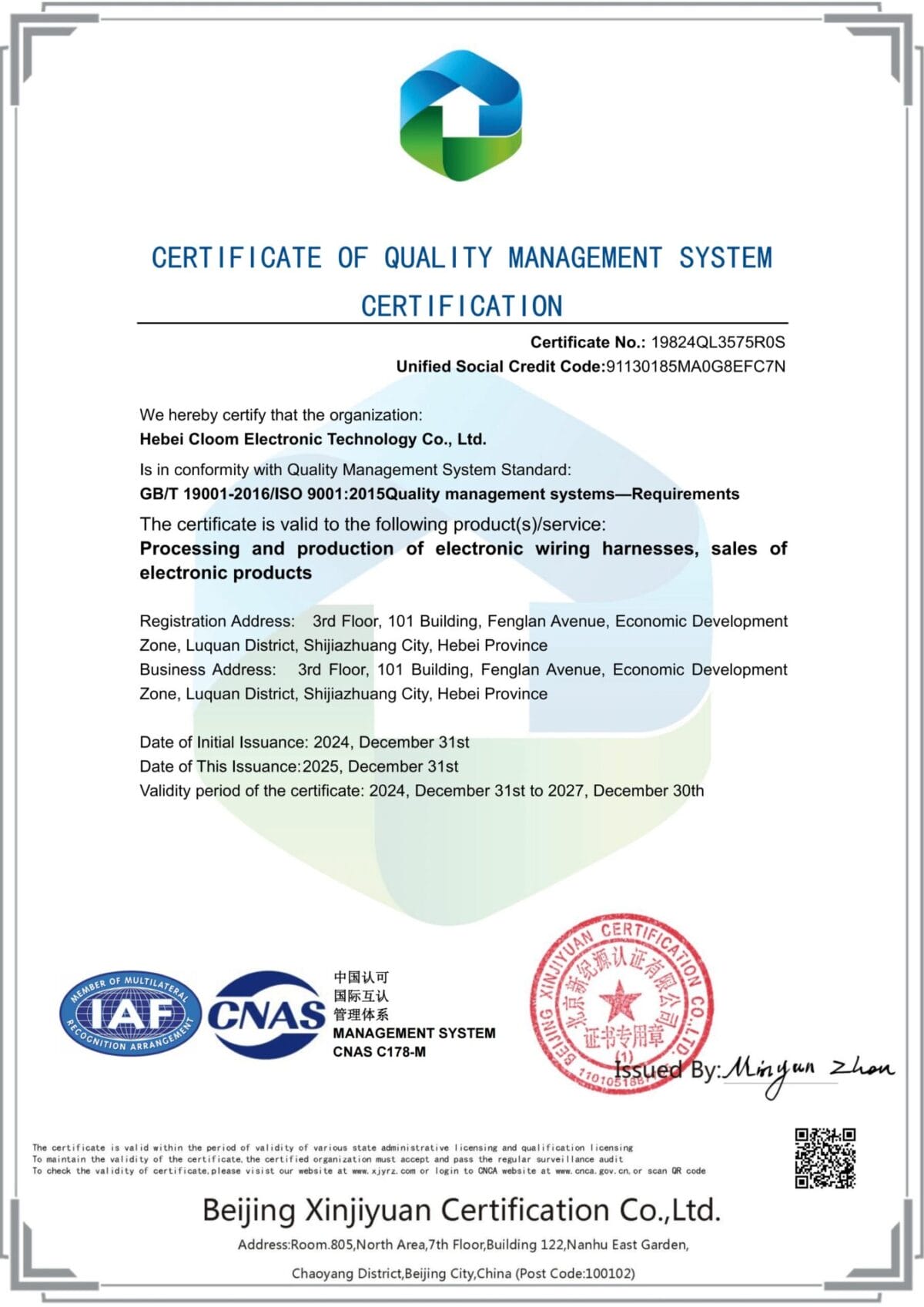
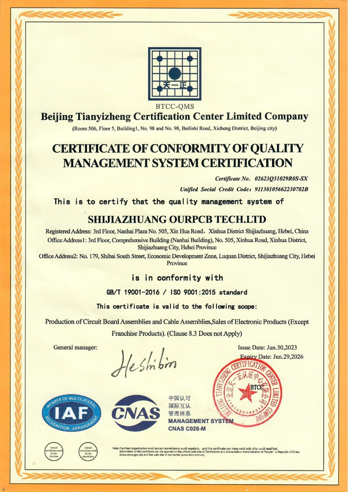
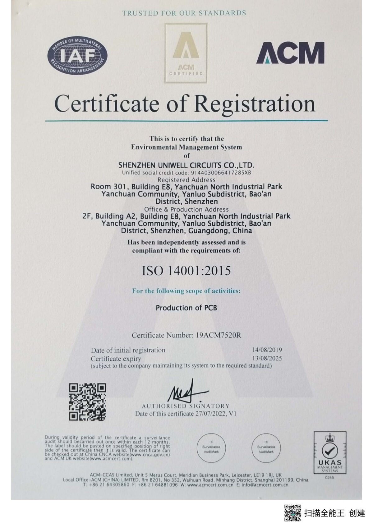
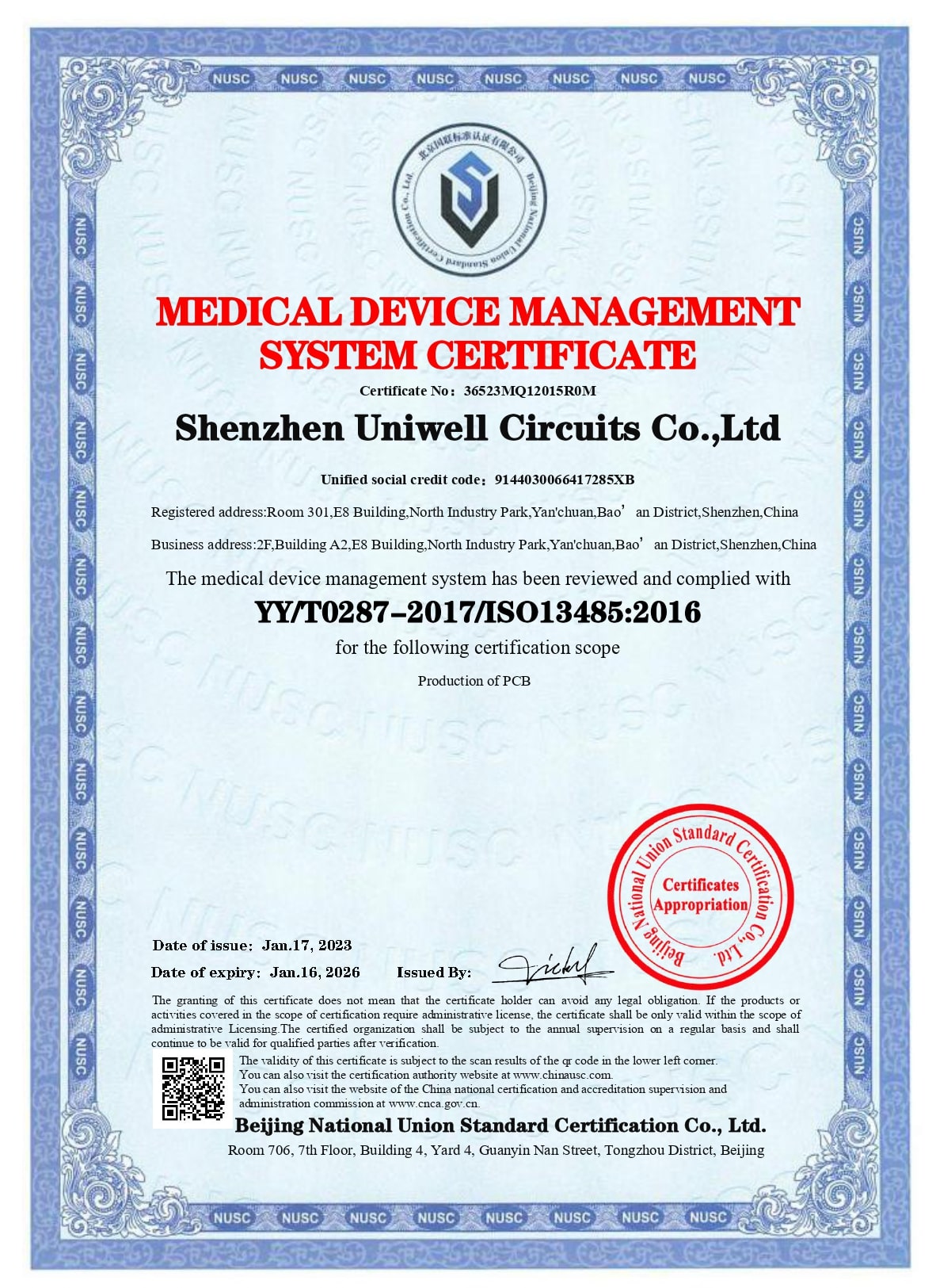
ISO9001 ISO13485
ISO14001

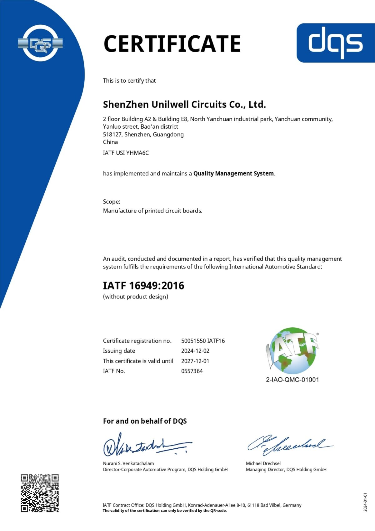
IATF
16949
IPC-A-610H International
Certification

Fully Automated
AOI Inspection

Extensive Experience As a Ceramic PCB Manufacturer

Complete Manufacturing Solutions

Superior Thermal Performance

Comprehensive Quality Control

Fast Prototyping and Scalable Production
Complete Design File Review

Aerospace Applications

Automotive Electronics

Medical Device Manufacturing

Telecommunications Infrastructure

Power Electronics & LED Systems

Operating Temperature Exceeds 300°F (150°C)

Power Density Exceeds 5 W/cm²

Frequency Exceeds 1 GHz

Size and Weight Constraints

Environmental Resistance Requirements

Submit Your PCB Design
Upload your Gerber files or use our easy online PCB design tool to create your board layout. Make sure your files are complete and correctly formatted to ensure smooth processing and production accuracy.

Select Your PCB Specifications
Customize your order by choosing the technical specifications—number of layers, board dimensions, thickness, copper weight, solder mask color, surface finish, and more. Our intuitive interface helps you configure everything based on your project’s needs.

Get an Instant Quote
Once your design and specs are in place, you'll receive a transparent, instant quote. Pricing updates in real time as you modify options, so you can adjust your selections to match your budget before placing the order.

Confirm Order & Make Payment
Review your entire order for accuracy, including file previews and selected specs. After confirmation, proceed to secure checkout and choose your preferred payment method. You’ll receive an email confirmation with order details.

Production & Delivery
Your PCB moves into production immediately. We’ll keep you updated throughout the manufacturing process. Once completed, your boards are carefully packed and shipped to your door, with tracking information provided for your convenience.


Hommer Zhao
Founder and Chief Editor – Hommer Zhao
Welcome! I’m Hommer Zhao, the founder and Chief Editor of WellPCB. With years of experience in the PCB industry, I’m committed to making sure our content is both accurate and helpful. We’re proud to serve a growing community of over 4,000 customers worldwide, and our goal is to provide you with the best resources and support. Your satisfaction is our top priority, and we’re here to help you every step of the way!

Jesse Holland
Technical Manager – Jesse Holland
Hi, I’m Jesse Holland, an Engineer and Technical Manager at WellPCB. With years of experience in PCB design and engineering, I’m here to ensure that every project we work on meets the highest technical standards. I lead our team, focusing on precision and innovation, collaborating closely with clients to provide tailored solutions and expert guidance. Whether you’re facing a complex design challenge or need advice on technical aspects, I’m here to ensure your project is a success from start to finish.

Nathan Jensen
Purchasing Manager – Nathan Jensen
Hi, I’m Nathan Jenson, the Purchasing Manager at WellPCB. I’m responsible for sourcing the best materials and components to ensure our products meet the highest quality standards. With my extensive experience in procurement, I work closely with suppliers to secure reliable and cost-effective solutions while maintaining strong relationships to support our operations. I aim to ensure every project runs smoothly by providing the resources needed to deliver on time and to your satisfaction.

Emma
Sales Manager – Emma
Hey, I am Emma, sales manager at WellPCB. I studied electronic science and technology at university and have served customers for PCB and PCB Assembly service for several years.
I enjoy communicating with customers and our technicians to solve problems, and customers always say, "It's great to have you onboard".
It is my pleasure and honour to be helpful. Contact me now, and you'll know.

Bella and Cassiel
Sales Representatives – Bella and Cassiel
We’re Bella and Cassiel, your dedicated sales representatives at WellPCB. With our extensive knowledge of the PCB industry, we’re here to provide exceptional service and support. We take the time to understand your unique needs and are always ready to offer tailored solutions and advice. Whether you need product recommendations, assistance with your orders, or simply have a question, we’re here to ensure your experience is smooth and seamless at every step.

Mandy and Wendy
Sales Representatives – Mandy and Wendy
We’re Mandy and Wendy, your friendly sales representatives at WellPCB. Passionate about helping our customers, we bring a wealth of experience in the PCB industry to provide you with the best solutions and service. We take pride in building strong relationships with our clients, understanding their specific needs, and offering personalised support to ensure their satisfaction. Whether you’re looking for advice, product information, or assistance with any part of your order, we’re here to make your experience as smooth and efficient as possible.
PCB Assembly
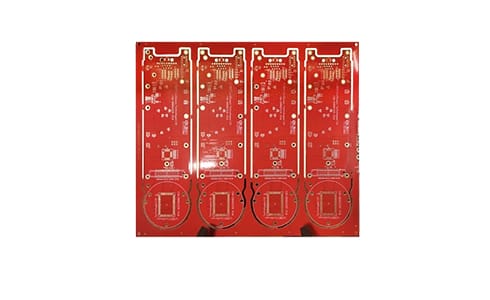
This red 8-layer board utilizes an immersion silver process and a TG170 substrate, offering excellent high-temperature resistance, solderability, and high-frequency performance. It facilitates the design of miniaturized, highly reliable circuits.
Features:
- •Immersion Silver/TG170
- •Hole copper: ≥20um
- •Min hole: 0.2mm
- •Surface copper: ≥35um
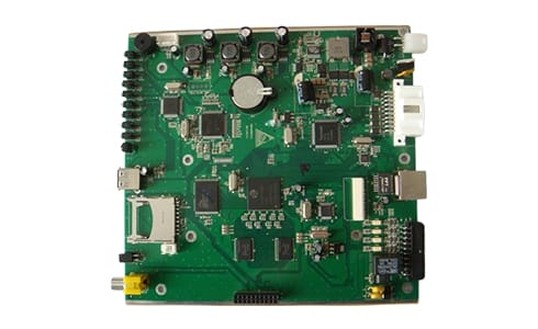
PCB Assembly
This 16-layer soldered PCB demonstrates exceptional performance and quality. Using Rogers laminate, it offers high-frequency performance and low loss, meeting the stringent signal integrity requirements of advanced fields like communications and radar. The thicker copper layer also provides a higher current-carrying capacity.
Features:
- •16-layer
- •Copper thickness: 3oz
- •Material: Rogers
- •Line Width / Line Space: 3 mil / 3 mil
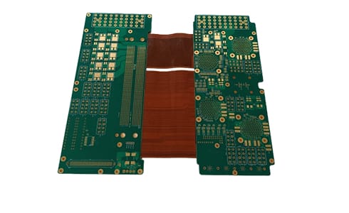
PCB Assembly
This 26-layer rigid-flex PCB is designed specifically for aerospace and military applications. Combining FR4 and PI materials, it provides both rigid support and flexible adaptability. With a thickness of 4.0mm ±10%, it features eight flexible layers and a layered design. With line widths and spacings of 4.5/6.0 mils, it meets the demands of high-density, high-precision circuits. Complying with military standards, it provides an efficient and stable circuit interconnect solution, ensuring stable operation of electronic systems in complex environments.
Features:
- •Material: IT180A+PI
- •Board thickness: 4.0mm
- •Features: 8 flexible layers
- •Min line width/space: 4.5/6mil
- •Application: Industry control